In this article, we use a SPICE model for 90 nm CMOS to plot key electrical relationships of an NMOS transistor.
In a previous article, I explained how to obtain an advanced SPICE model for integrated-circuit MOSFETs and incorporate it into an LTspice simulation. We then used this model to investigate an NMOS transistor’s threshold voltage. In this article, we’ll use the same model to generate plots that visually convey the transistor’s electrical behavior.
Plotting Drain Current vs. Drain Voltage
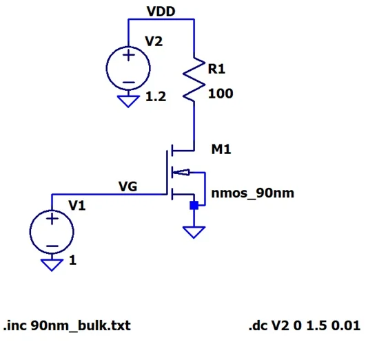
We’ll start by producing a basic plot of drain current (ID) versus drain-to-source voltage (VDS). To do this, we’ll set the gate voltage to a fixed value that’s well above the threshold voltage, then perform a DC sweep simulation in which the value of VDD gradually increases. Figure 1 shows the schematic we’ll use.

Figure 1. LTspice schematic of a basic NMOS transistor. We’ll use it to produce a drain current vs. drain voltage curve.
The gate-to-source voltage (VGS) of 1 V is comfortably higher than 320 mV, the threshold voltage we found through simulations in the previous article. Meanwhile, the .dc simulation command at the bottom right of Figure 1 tells LTspice to do two things:
- Increase the V2 source (VDD) from 0 V to 1.5 V in 0.01 V increments.
- Use this series of VDD values as the independent variable.
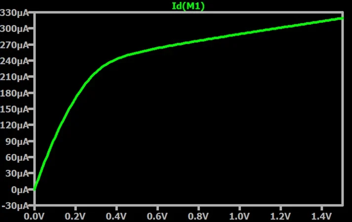
The results of our simulation can be seen in Figure 2.

Figure 2. Our initial plot of drain current vs. drain-to-source voltage.
The gate voltage is high enough to enable conduction, so current starts to flow as soon as VDS increases past zero. With lower drain voltages, drain current increases linearly in response to the linear increase in VDS. However, drain current starts to level off at about 0.4 V and increases more slowly thereafter. This transition from the higher-slope portion of the graph to the lower-slope portion corresponds to the transition from the FET’s linear region to its saturation region.
When the drain voltage is low, the gate voltage opens a channel that extends from drain to source and current flows more freely through the FET’s channel. As the drain voltage approaches the overdrive voltage, the channel at the drain is pinched off and current no longer flows as freely as before. The overdrive voltage is equal to the gate voltage minus the threshold voltage.
Measuring Resistance in the Linear Region
An NMOS in the linear region behaves like a voltage-controlled resistor. That’s what gives the region its name—when current is flowing through ordinary resistance, the relationship between voltage and current is linear. This is apparent if we look at Ohm’s law:
V = IR𝑉 = 𝐼𝑅
If we replace V, I, and R with the letters that many of us used back in high-school algebra, Ohm’s law becomes:
y = mx𝑦 = 𝑚𝑥
where:
y, the vertical axis, is voltage
x, the horizontal axis, is current
m, the slope of the plotted line, is resistance.
To determine the resistance of this NMOS transistor in the linear region, we just need to find m. Since we plotted the relationship between drain current and drain voltage in Figure 2, we’re already partway there. However, we plotted current on the y-axis and voltage on the x-axis—for V = IR to work, voltage must be a y value and current must be x. Rather than being the slope of the line in Figure 2, m is the slope’s inverse.
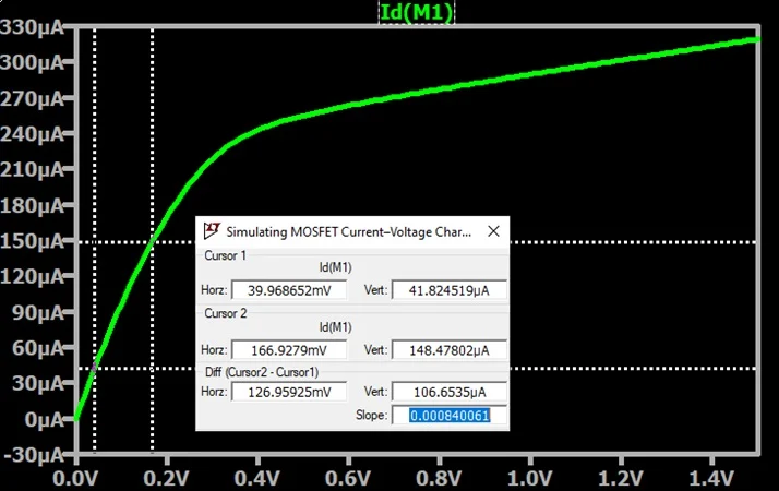
This only adds one extra step. We use LTspice to find the slope (Figure 3), then take the inverse.

Figure 3. Finding the slope of the drain current vs. drain voltage curve in the FET’s linear region.
The slope of the line is 0.00084. Total resistance is therefore 1/0.00084 = 1190 Ω. This total resistance includes a 100 Ω drain resistor, making the channel resistance of the NMOS equal to 1090 Ω.
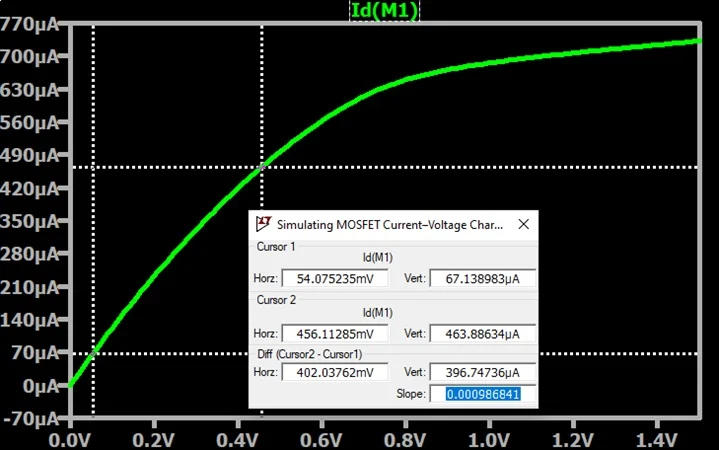
Higher gate-to-source voltage makes the channel more conductive, so we can expect this resistance to decrease if we increase the gate voltage. Figure 4 shows what happens if I increase the gate voltage to 2 V.

Figure 4. The slope of the drain current vs. drain voltage curve once gate voltage is increased to 2 V.
With VGS = 2 V, the slope is equal to 0.00099. Taking the inverse of this value gives us 1010 Ω. Once we subtract the 100 Ω drain resistor, the FET’s channel resistance in the linear region is 910 Ω. That’s a decrease of 180 Ω from our previous resistance value, so we can consider our expectation confirmed.
Generating a Set of Characteristic Curves
Discussions of FET behavior are often accompanied by a drain current vs. drain voltage plot that includes multiple curves to represent results for different gate-to-source voltages. This allows a single plot to convey a great deal of information about the electrical relationships between gate-to-source voltage, drain-to-source voltage, and drain current.
To generate this type of plot in LTspice, we just need to modify the simulation command so that it specifies a sweep for both V2 and V1 (which is the gate voltage). The new simulation command is:
.dc V2 0 1.5 0.01 V1 0 3 0.5
The V2 sweep is the same as before, but we’ve added text that tells LTspice to increase the V1 source from 0 V to 3 V in 0.5 V increments. The result is the multicolored plot in Figure 5.

Figure 5. Drain current vs. drain voltage for seven different values of gate voltage.
To make your plot display a legend like Figure 5, just follow these steps:
- Right-click on the plot window.
- Go to View.
- Select Step Legend.
Wrapping Up
SPICE simulations are a great way to learn more about MOSFETs and to investigate subtle electrical details or complex circuit implementations. The advanced models available for free from the Predictive Technology Model website allow us to maintain simulation accuracy even when we’re working with MOSFET technologies used in modern integrated circuits.

